Material coating
For more than a decade, material coating has been an essential core competence at the FHV. Dry etching using Deep Reactive Ion Etching (DRIE) and coating using Physical Vapor Deposition (PVD) in particular are important pillars of our research and development efforts.
Dry Etching, (D)RIE - (Deep) Reactive Ion Etching
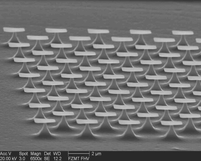
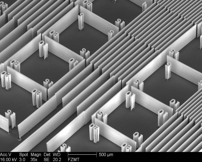
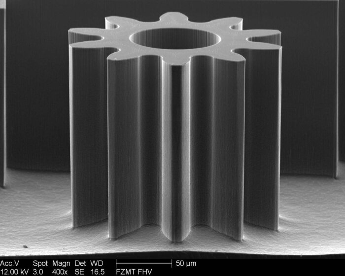
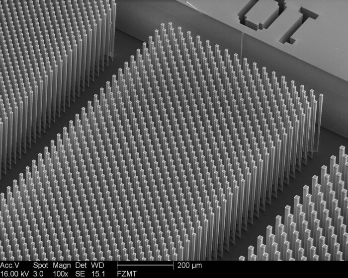
With adixen's DRIE - system "AMS 100 i-Speeder" smallest topographic structures for micro and nano system technology can be fabricated, preferably on silicon wafers). DRIE includes both chemical and physical etching mechanisms, the respective proportions of which can be precisely controlled, so that isotropic (direction-independent) and also anisotropic (directional) etchings are possible. Geometric structuring of the wafer surface is provided by masking applied lithographically before the start of the process. RIE delivers very good results even for very fine structures with dimensions well below 100 nm. DRIE (Deep Reactive Ion Etching) is an RIE modification for deep etching of silicon ("Bosch™ process"). With this method, the highest aspect ratios can be achieved.
Some application examples:
-
Micro- and nanometer-scale structures for electrochemical biosensors
-
Manufacturing structures for microfluidic systems
-
Structures for micro-electromechanical systems (MEMS)
-
Manufacture of stamps for impression with polymer materials (casting, injection molding)
Specifications:
-
Wafer size: 100 mm
-
Etch depth: max. 500 µm
-
Aspect ratios (width / depth): max. 1:60 (depending on material)
-
Resolution: better 100 nm (mask dependent)
Services:
-
Structuring of wafers by means of RIE or DRIE
-
Feasibility tests in the field of Si structuring
Coating (Physical Vapor Deposition - PVD)
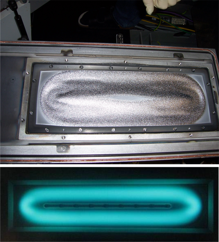
PVD coating enables the deposition of thin films with thicknesses ranging from a few nanometers to a few micrometers on a wide variety of - preferably flat ("2D") - substrates and surfaces. To carry out the vacuum-based processes required for this purpose, two technology variants are available at the FZMT, namely thermal evaporation and sputtering (i.e. "cathode sputtering"), which are very flexible with regard to the selection of the coating material and thus enable the deposition of a wide variety of coatings.
Some application examples:
-
Metallizations for lift-off processes
-
Starting layers for electroplating processes
-
Masking for RIE / DRIE processes
-
Insulating / dielectric layers
-
Multi-layer layer stacks of different materials
Specifications:
Thermal Vapor Deposition - Balzers BAK 550
-
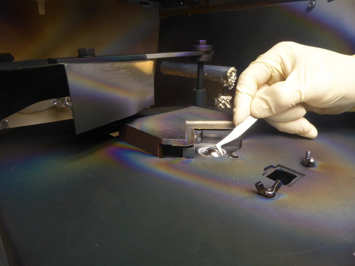
Evaporation source: 10 kW electron beam evaporator with 4-pass crucible,
enables the evaporation of almost any material,
-
Real-time monitoring of coating thickness using oscillating quartz oscillator (accuracy better than 1nm)
-
Maximum substrate size: 160 x 160 mm (L x W), other sizes + shapes by arrangement
-
Process temperature: 50 - 200 °C
-
Layer thicknesses: 5 nm - 500 nm
Sputtering - Oerlikon LLS EVO
-
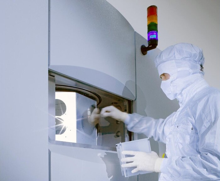
Two-chamber sputtering system with recipe-based automatic process control
-
Substrate pretreatment (bakeout up to 120 °C, plasma cleaning) possible in process
-
5 Planarmagnetron sputtering sources, power: max. 5 kW pulsed DC (0 - 350 kHz)
-
Sputter modes: metal mode (Ar as process gas), reactive mode (O2 or N2 addition)
-
Standard available coating materials: Al, Cu, Ti, Ni, Si, Cr, Al2O3, TiO2, SiO2, Si3N4
-
Maximum substrate size: 150 x 250 mm (L x W), other sizes + shapes by arrangement
-
Process temperature: ≈ 50 °C during coating
-
Coating thicknesses: 10 nm - 1 µm
Services:
-
Single piece and test coating of substrates according to customer's requirement
-
Support + advice on material selection and process development for PVD coatings


