Laser processing
The fabrication and transfer of microstructures are among the most important tasks in applied research and industrial development. By means of optical lithography and laser micromachining, we enable mechanical fine machining and are continuously opening up new manufacturing fields in the micro area.
Optical Lithography
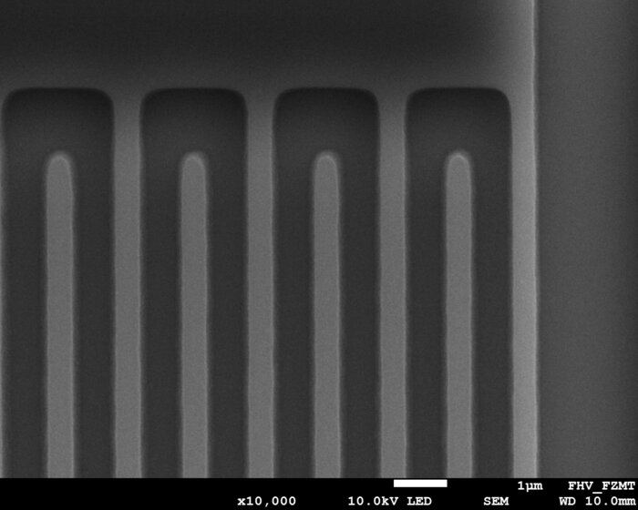
Optical lithography is one of the most important methods for the fabrication and transfer of microstructures, in which a pattern specified on a mask is transferred to a substrate. For this purpose, a light-sensitive photoresist (resist) is applied to the carrier material (substrate) and exposed to UV light through the mask. Due to a change in the crosslinking of the photoresist in the irradiated areas, selective dissolution of the resist can be achieved in a subsequent development step. Structures of resists with different properties (high chem. resistance, easy solubility...) and with layer thicknesses from 100 nm up to 0.6 mm are possible. Multilayer, superimposed structures can also be created. In addition to classical mask lithography, exposure can also be made by a direct-writing laser beam or electron beam. In this case, no mask is necessary and therefore predestined for process development.
Some application examples:
-
Structuring for thin film technology (lift-off)
-
Masking for dry etching and wet chemical etching
-
Direct manufacturing of microdevices
-
Stamp fabrication for impressions
Specifications:
-
Automatic processing of substrate sizes up to 200mm (100mm, 200mm)
-
Automatic belacker and developer SUSS ACS200
-
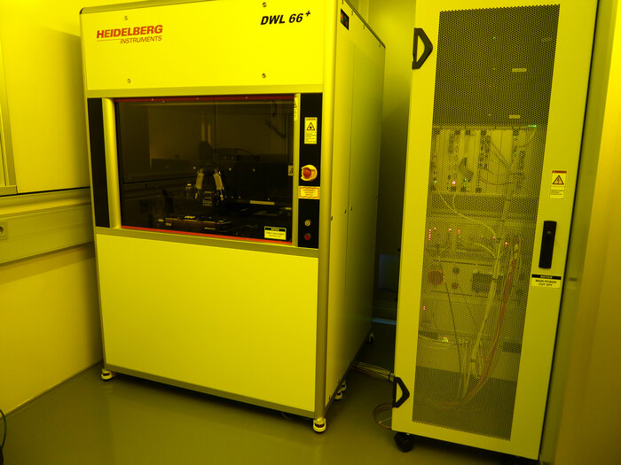
Heidelberg Instruments DWL66+ (resolution up to 700nm line and space possible)
-
Maskaligner MA6
-
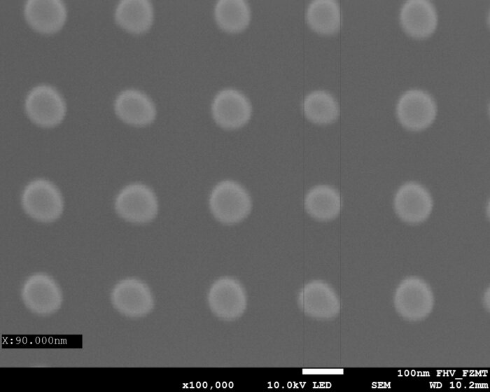
Xenos e-beam patterning generator XeDraw 2 (resolution < 100nm possible)
Services:
-
Paintings and exposures of different substrate sizes
-
Support and consulting on lithographic issues and new process developments
Contact
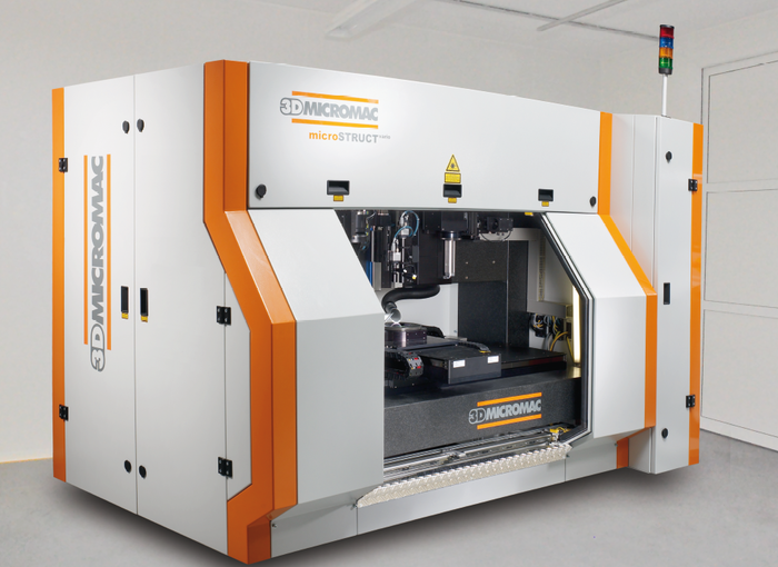
Laser Micromachining System microSTRUCTTM vario (3D Micromac AG)
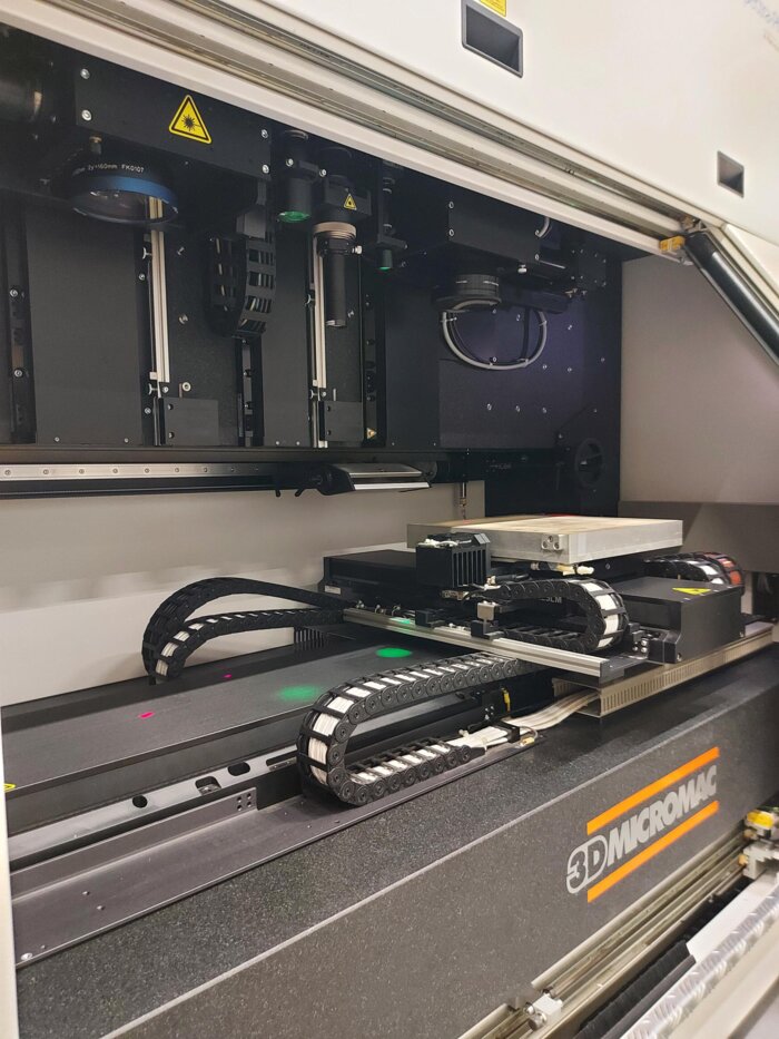
The laser micromachining system microSTRUCTTM vario is ideal for activities in applied research as well as industry-related development. It is equipped with a femtosecond laser (Spectra Physics) of the latest generation. This can be operated at three different wavelengths, depending on the application. Depending on the application, processing with scanners as well as with fixed optics allow the best possible technical implementation of the processes to be developed.
Femtosecond laser processing enables precise and material-friendly cutting, drilling of holes of almost any cross-section, as well as the production of three-dimensional surface structures and smallest parts.
The machining of a wide variety of materials, such as soft plastics, hard metals, glasses, sapphire or diamond is possible. Mechanical fine machining processes are complemented by laser ablation to open up new manufacturing fields in the micro range.
Specifications:
Beam paths
microSTRUCTTM vario is equipped with three working areas, two scanners and one fixed optics,
Scanner 1: Processing with wavelengths of 1035 nm and 518 nm
Scanner 2: processing with the wavelength 345 nm
Fixed optics: Precise processing by strong focusing with 1035 nm
Positioning system
xy axes (Aerotec)
Travel 800 mm x 400 mm
Positioning accuracy x- / y-axis: ± 2 µm / ±2 µm
Repeat accuracy x- / y-axis: ± 2 µm / ±1 µm
Laser
Ultra-short pulse laser Spirit© (Spectra Physics)
Wavelengths: 1035 nm / 518 nm / 345 nm
Pulse duration: <400 fs
Output power: 30 W (max @ IR)


